Our SEM-EBSD detector is dedicated to the microstructural analysis of crystalline materials, especially metals: solder joints for electronic assemblies and additive manufacturing parts (TA6V, AS7, Inconel, stainless steels…). Alternative analyses, by optical inspection, may be performed : grains revelation after chemical etching grain revelation by chemical etching or under polarized light.
Failure analysis: identification of the metallurgical phenomenon that contributed to a damage (thermomechanical wear, growith of fragile IMC…)
R&D: determination of the physical and metallurgical aging mechanisms (recrystallization / grain growth ; granular rotation ; IMC coalescence ; stress relaxation) and their kinetic, depending on thermal profiles
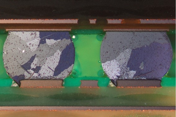
We mostly analyze electronic solder joints, leadfree ( SAC305, AuSn, SnSb...) or leaded (SnPb, SnPbAg). Beyond these materials, SEM-EBSD is useful on various materials: semiconductors, additive manufacturing metals, ceramics.
SEM-EBSD on electronic solder joints
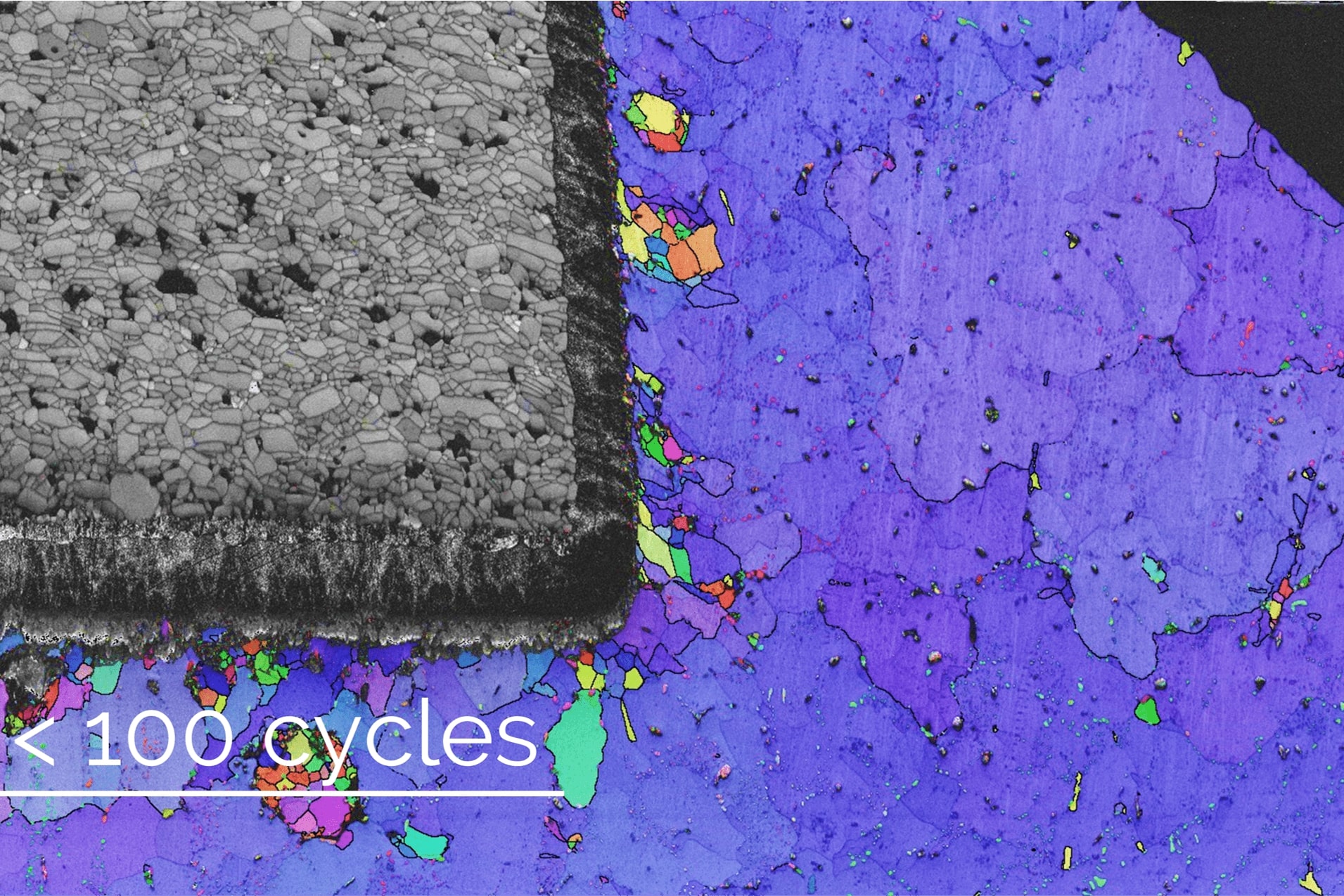
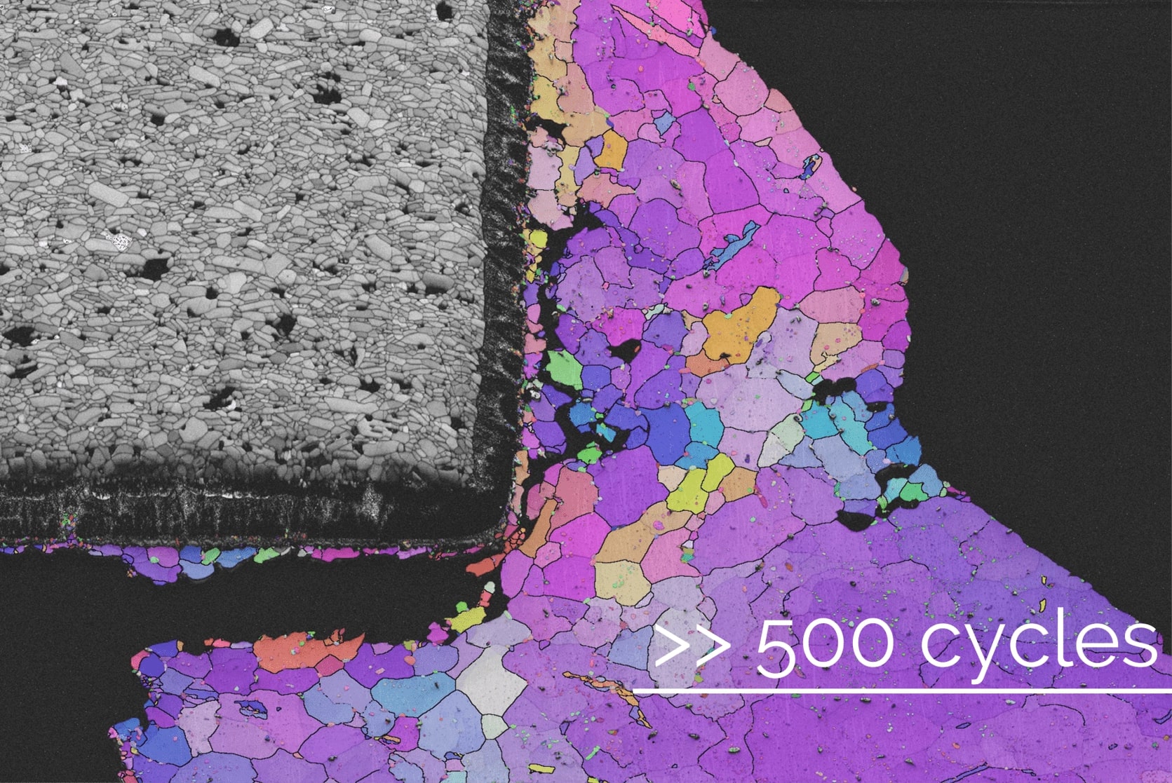
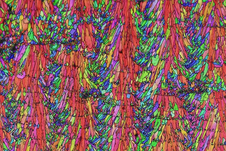
EBSD maps of a SAC solder joint, after microsection :
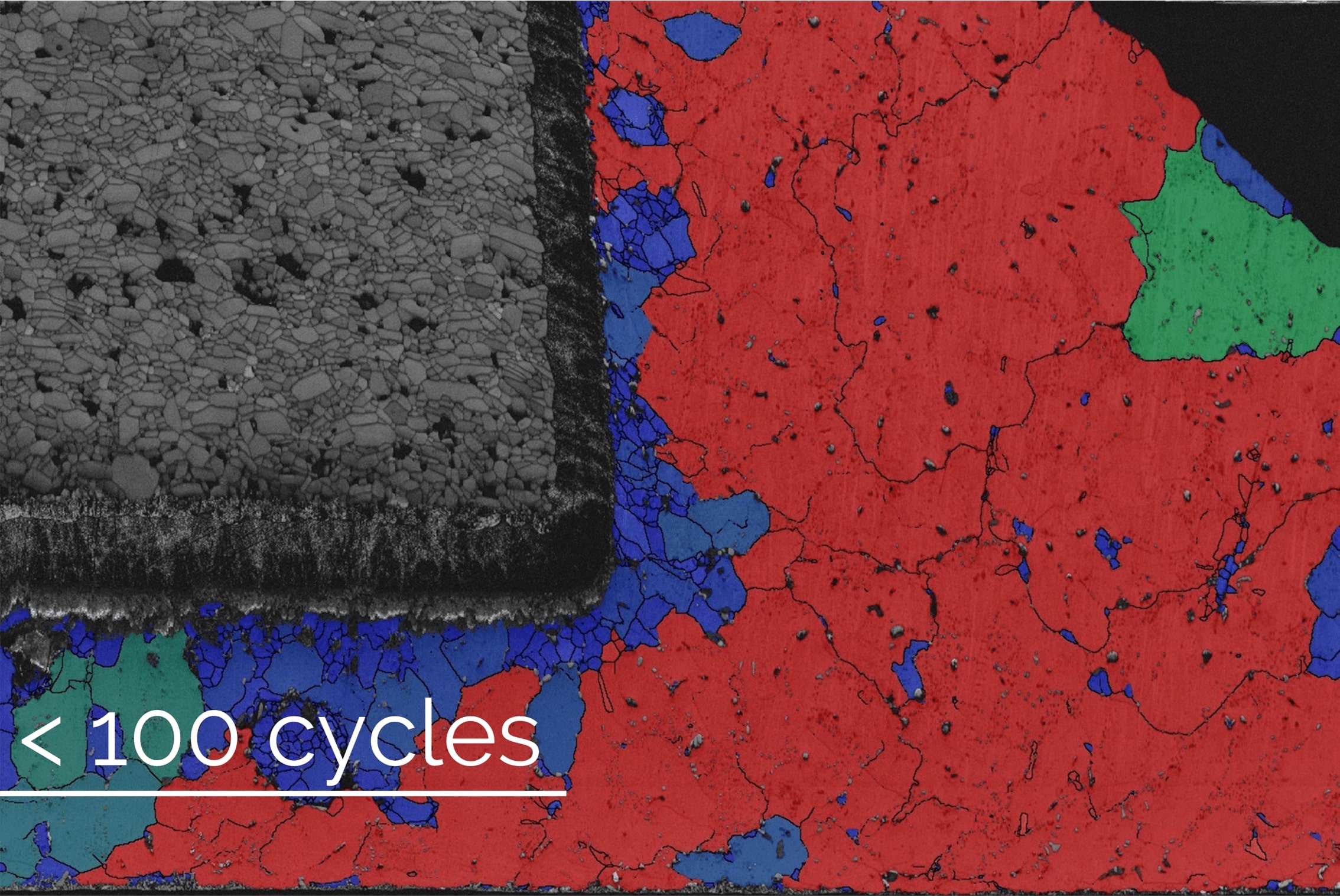
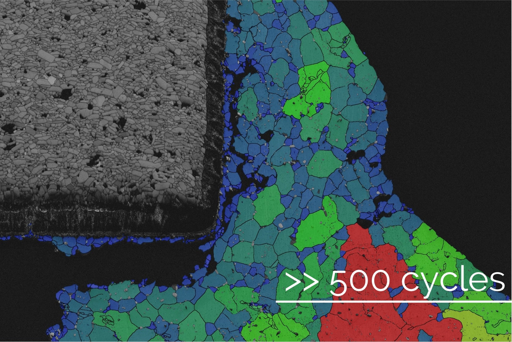
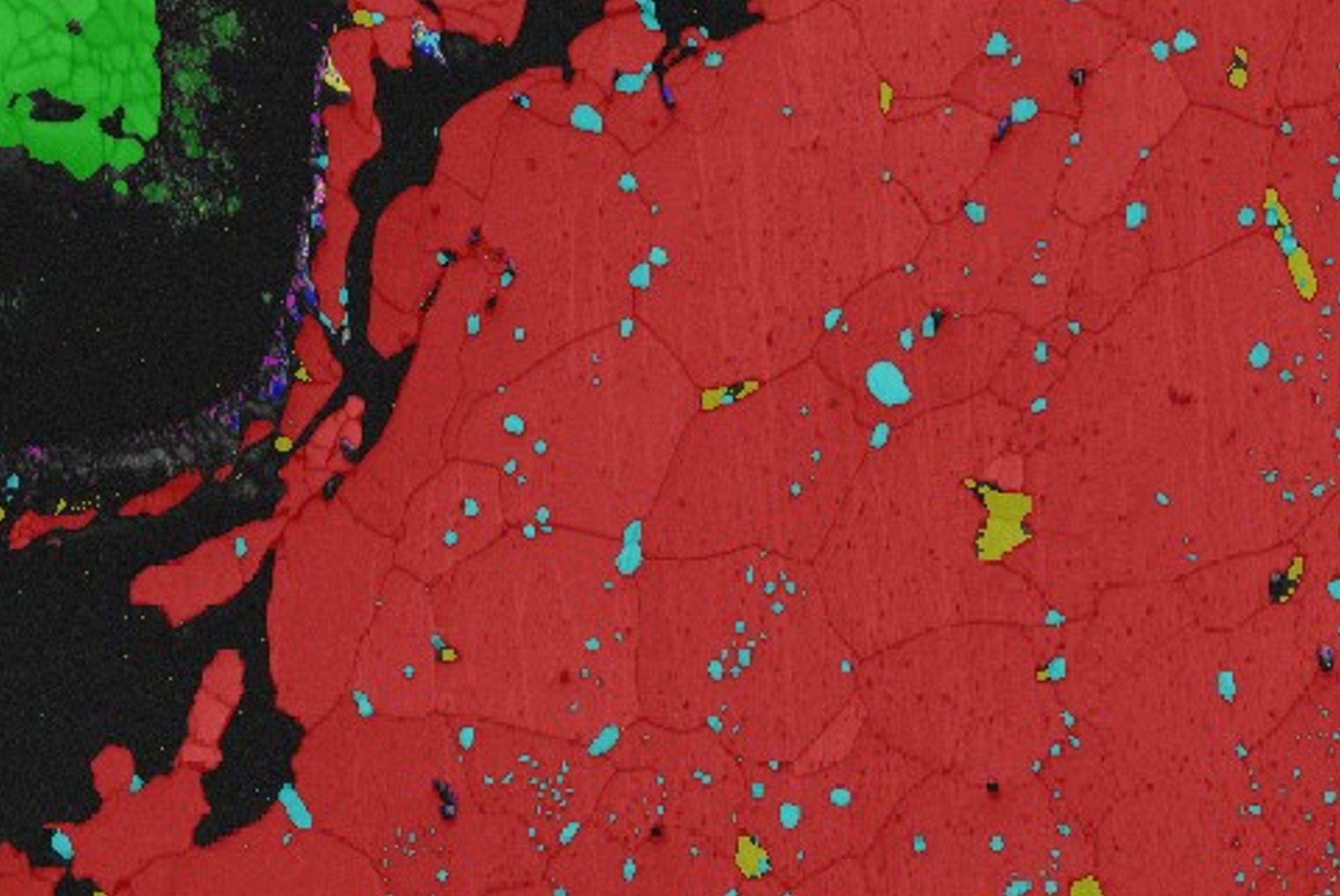
Granulometry (grain size & shape)
→ recrystallization & grain growth
Grain orientation & texture (MUD)
→ anisotropy
Précipitates, IMC & phase discrimination
→ coalescence of IMC & phase ratio
Permanent strain (intragranular disorientation)
→ mechanical damage
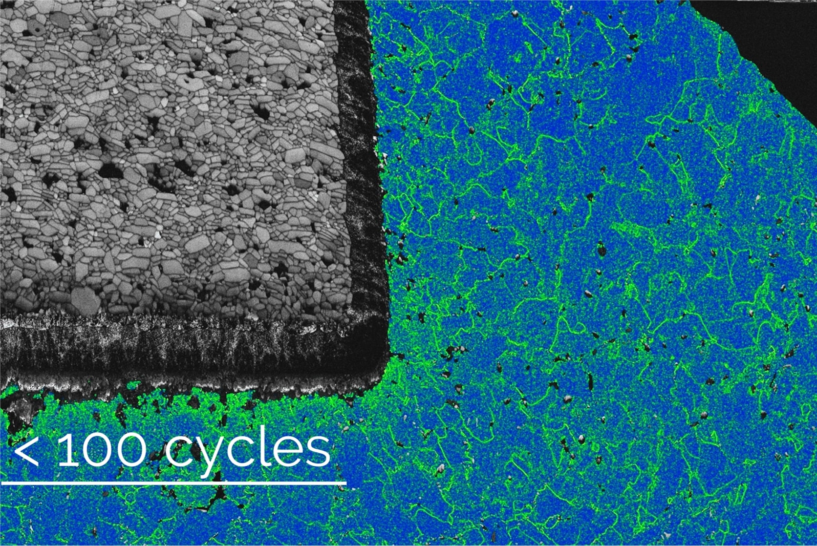
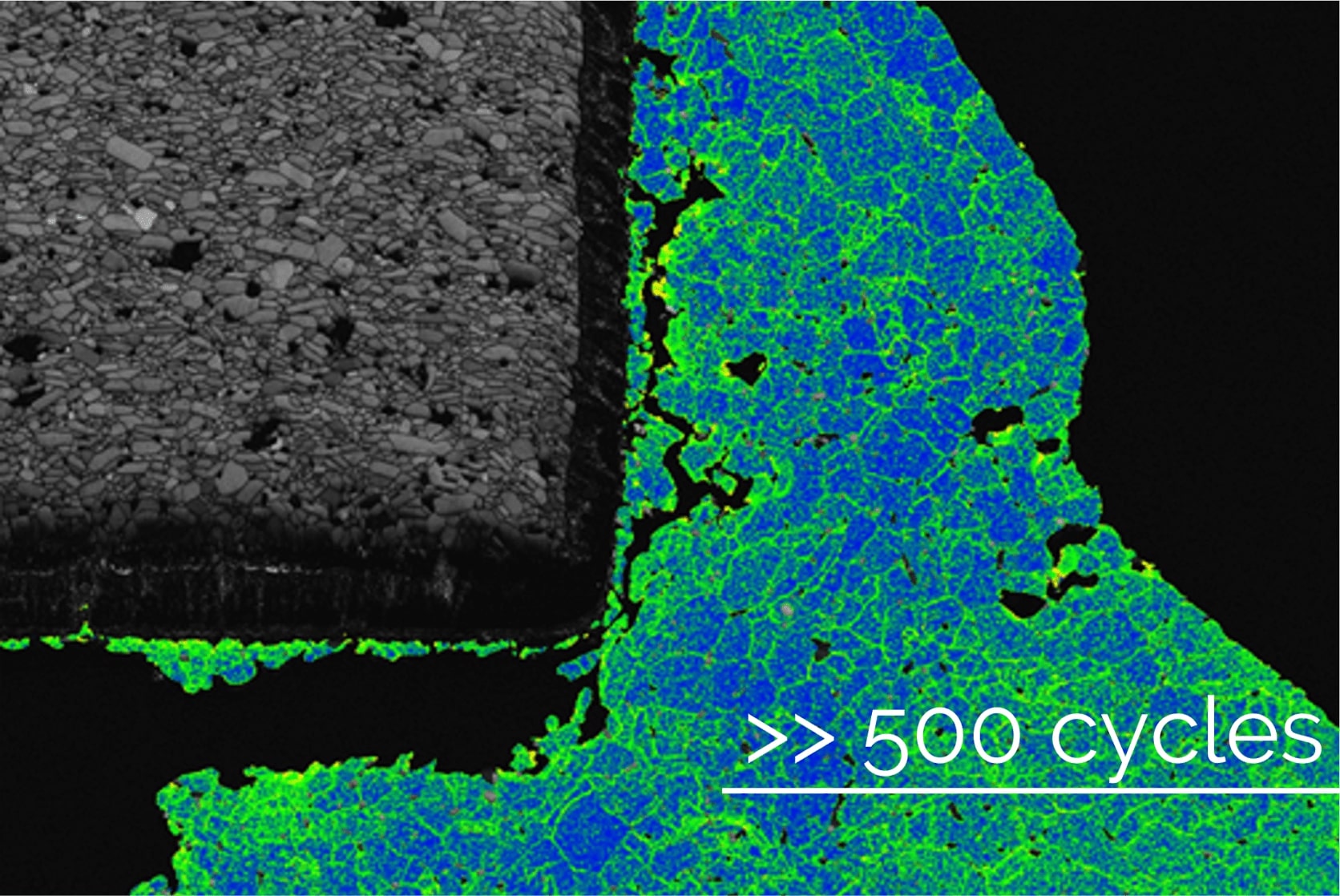
SEM-EBSD on additive manufactured part
EBSD mapping on LBM-processed AS7 :
Visualization of the laser path (SEM-EBSD in top-view)
Grain shape (SEM-EBSD on microsection)
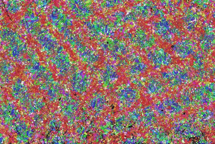
Optical inspections
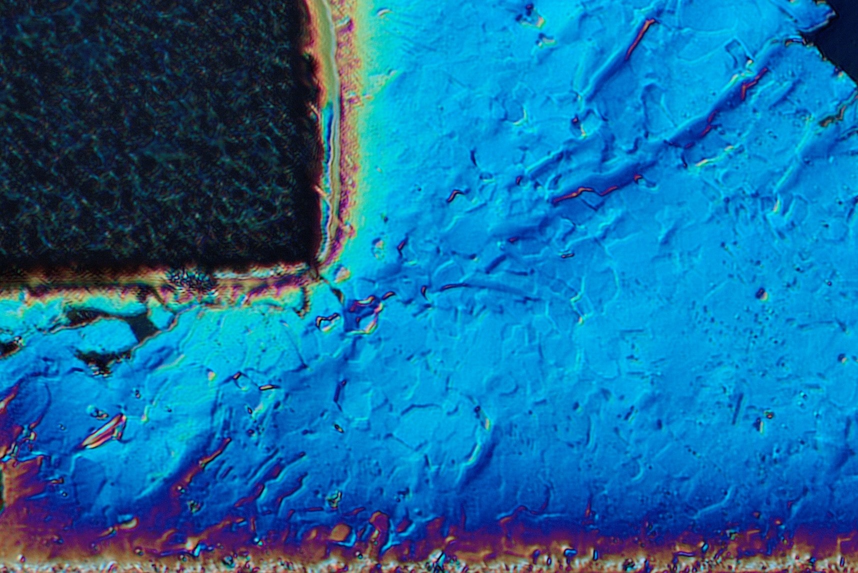
Topography (NIC : Nomarski interference contrast)
Observation of the grain orientation (polarized light, after chemical revelation)
Do you want a detailed presentation of our Lab services or consult us on a specific need ?