
The physical analysis of technologies and materials is our core business. We use various techniques to extract the characteristics of the structures and materials, in order to highlight the failure mechanisms or the design / manufacturing choices :
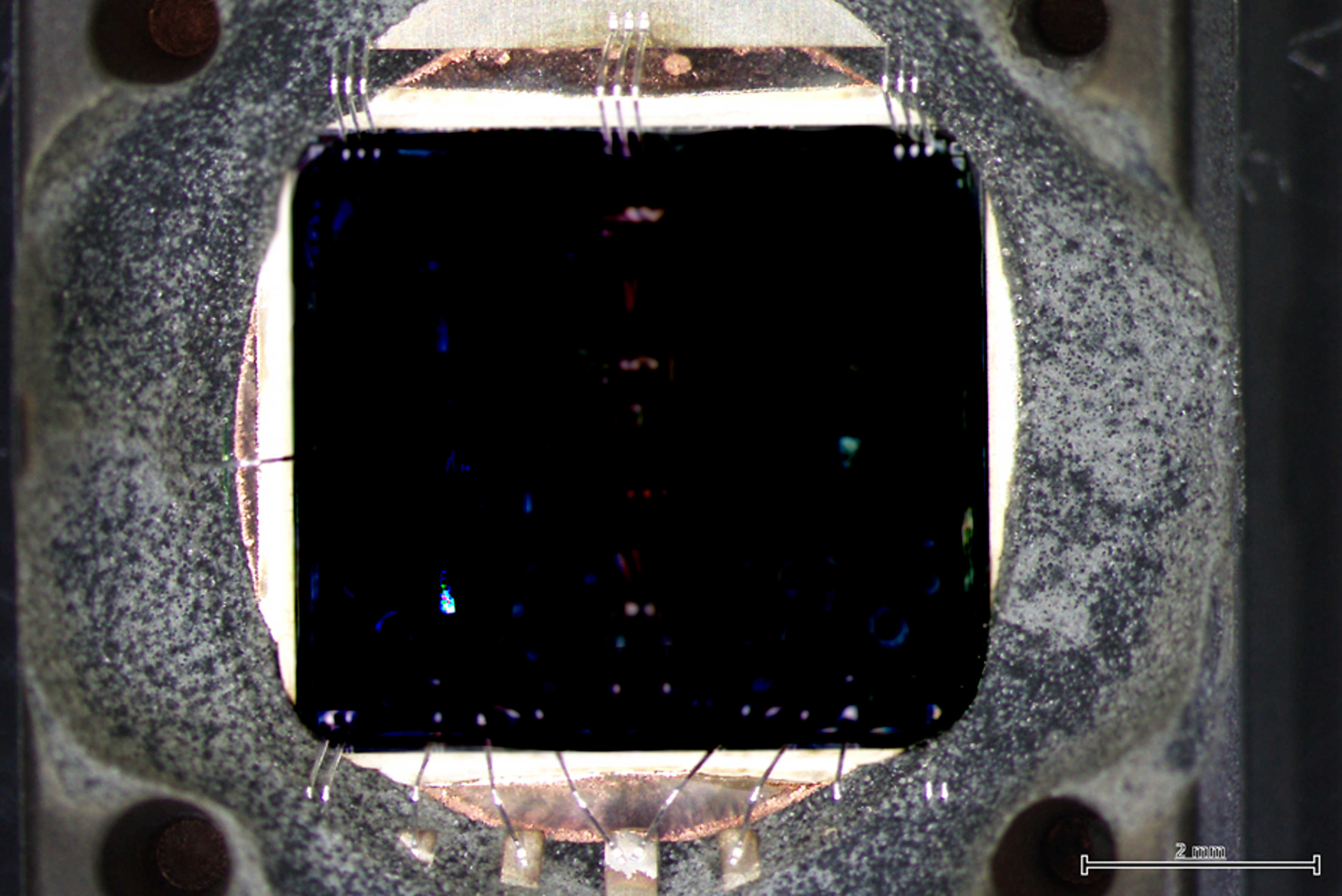
Failure analysis: defect characterization (morphology, chemical composition), after its preliminary non-destructive localization
Reverse engineering or process control (front-end + back-end): dimensional measurements and identification of materials
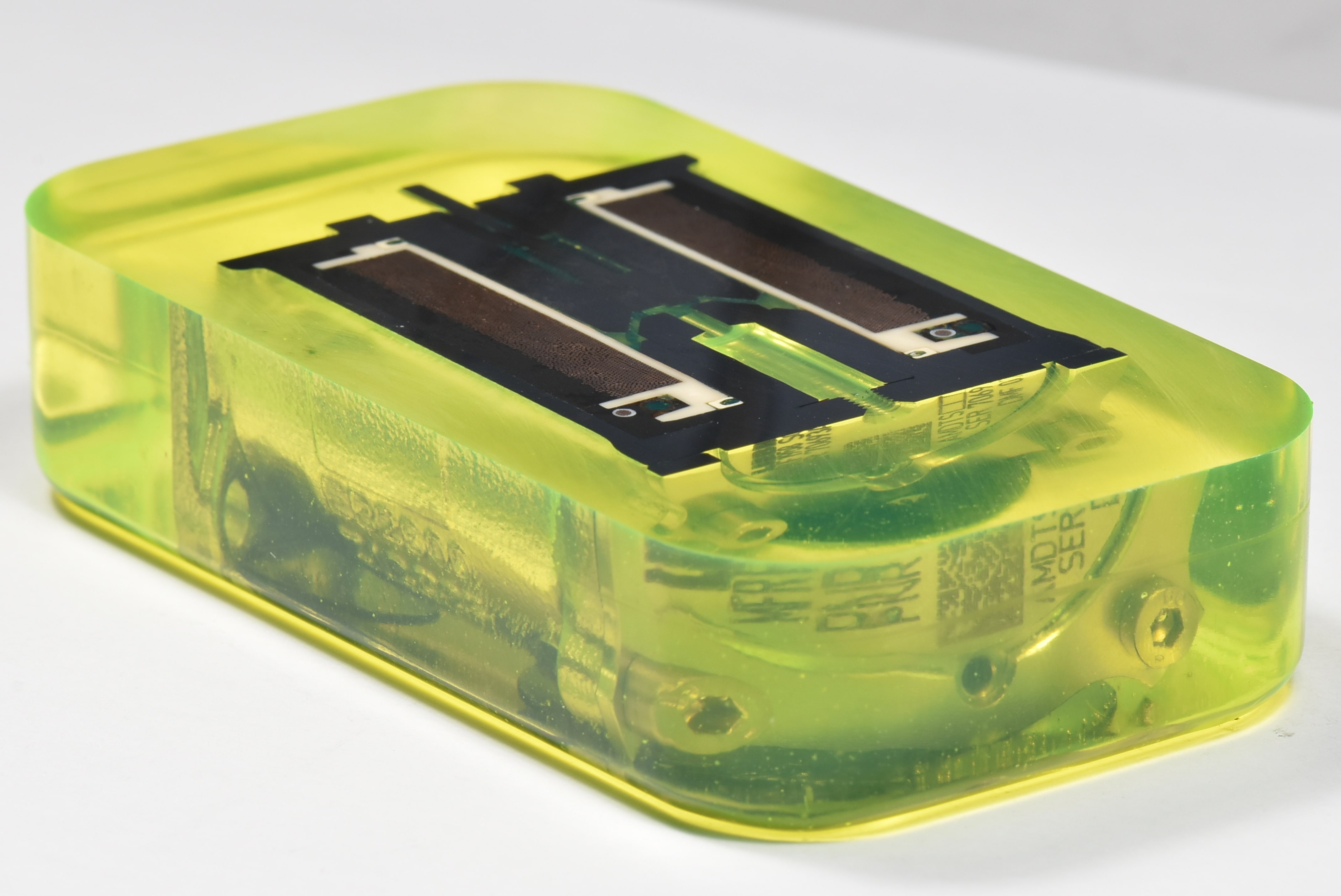
Quality assessment of the assembly (PCBA): integrity of solder joints (IPC-A-610 visual inspections, ECSS-Q-ST-70-38C optical microscopy on microsections
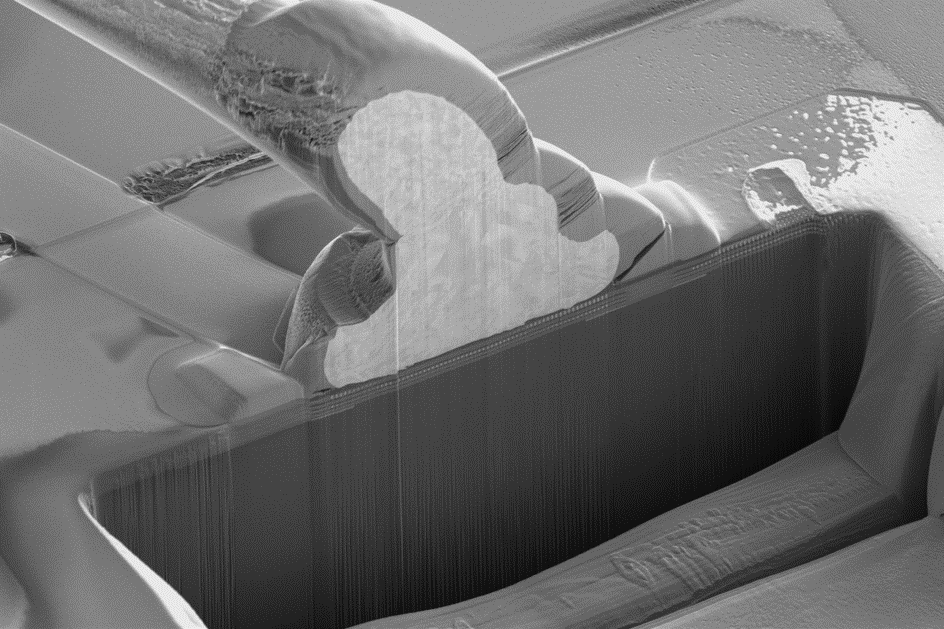
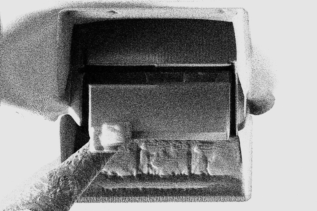
Mechanical damage: fractographic or contamination analysis
These surface or in-depth analyses address a wide range of technologies: circuit boards, interconnects, singulated or on-wafer components and mechanical parts.
Two key features are performed to succeed: sample preparation (access to the area of interest) + imaging / surface analysis (inspection and material characterization).
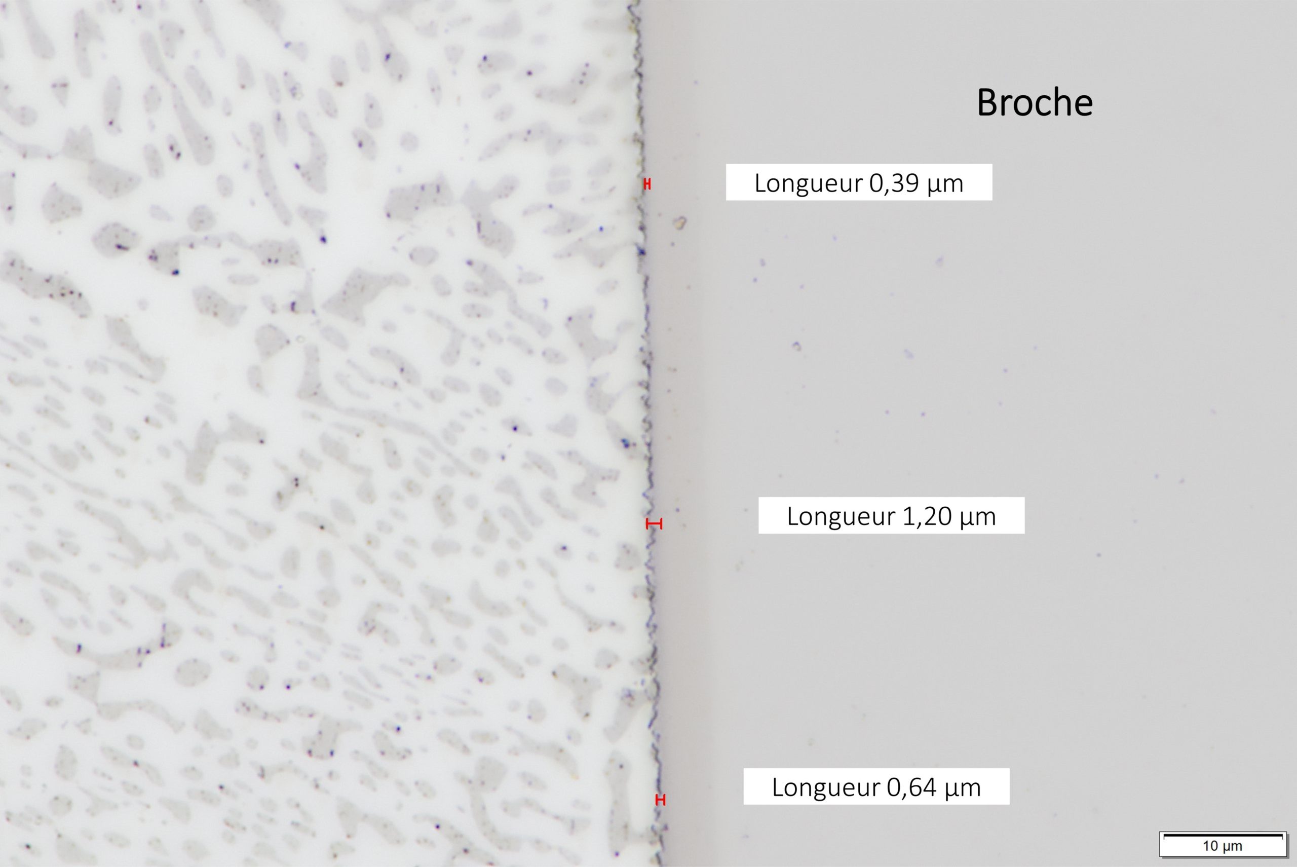
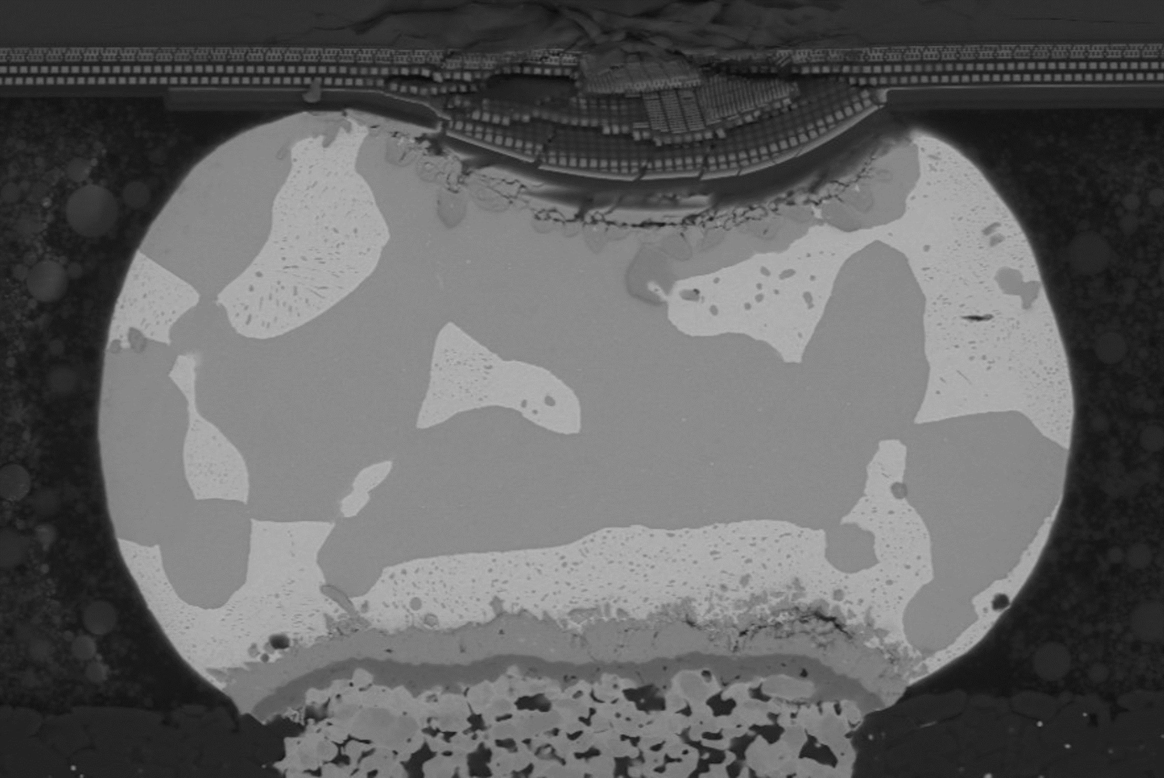
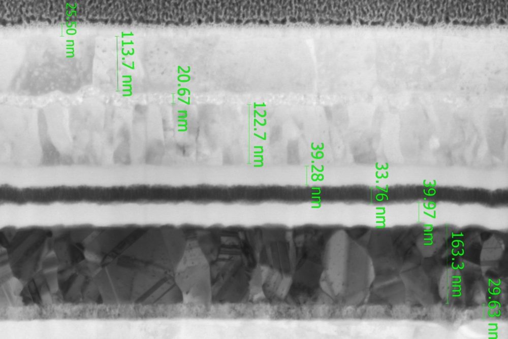
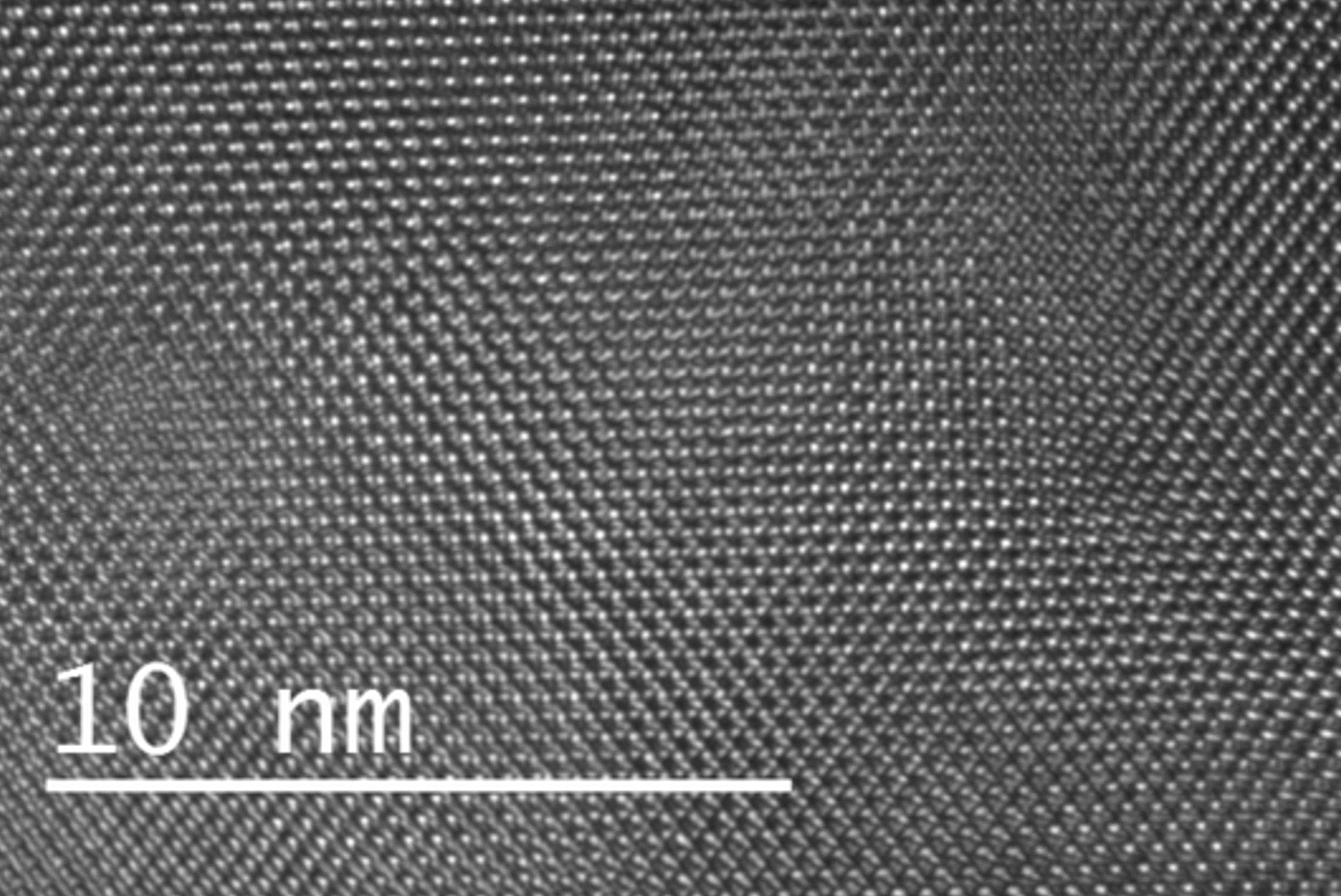
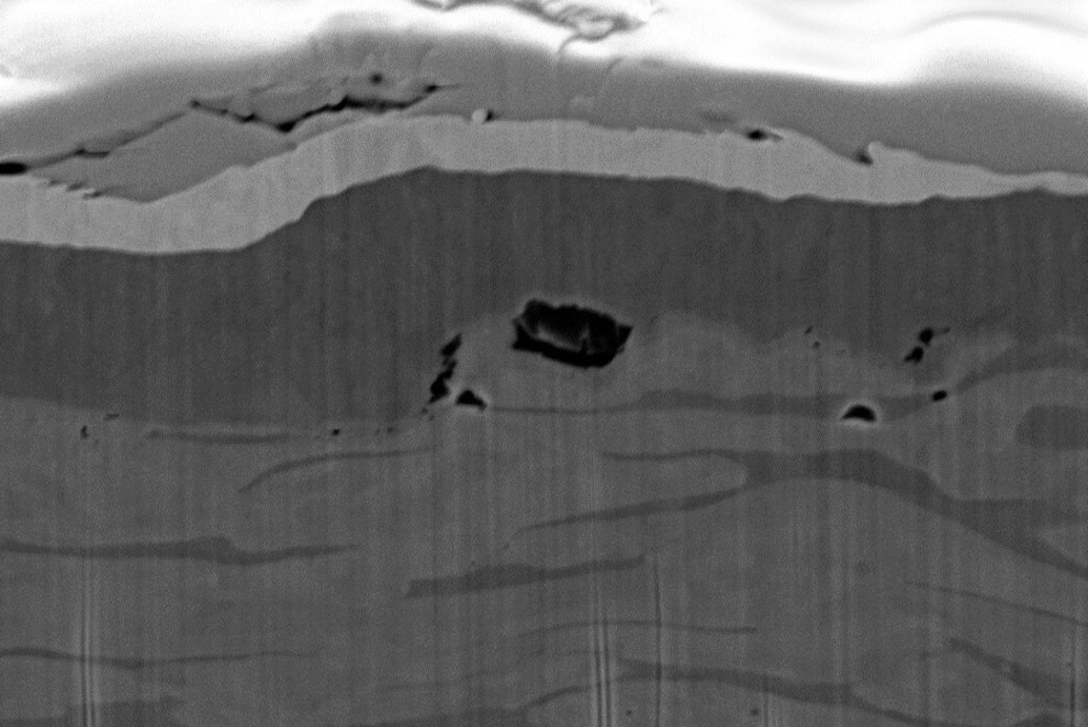
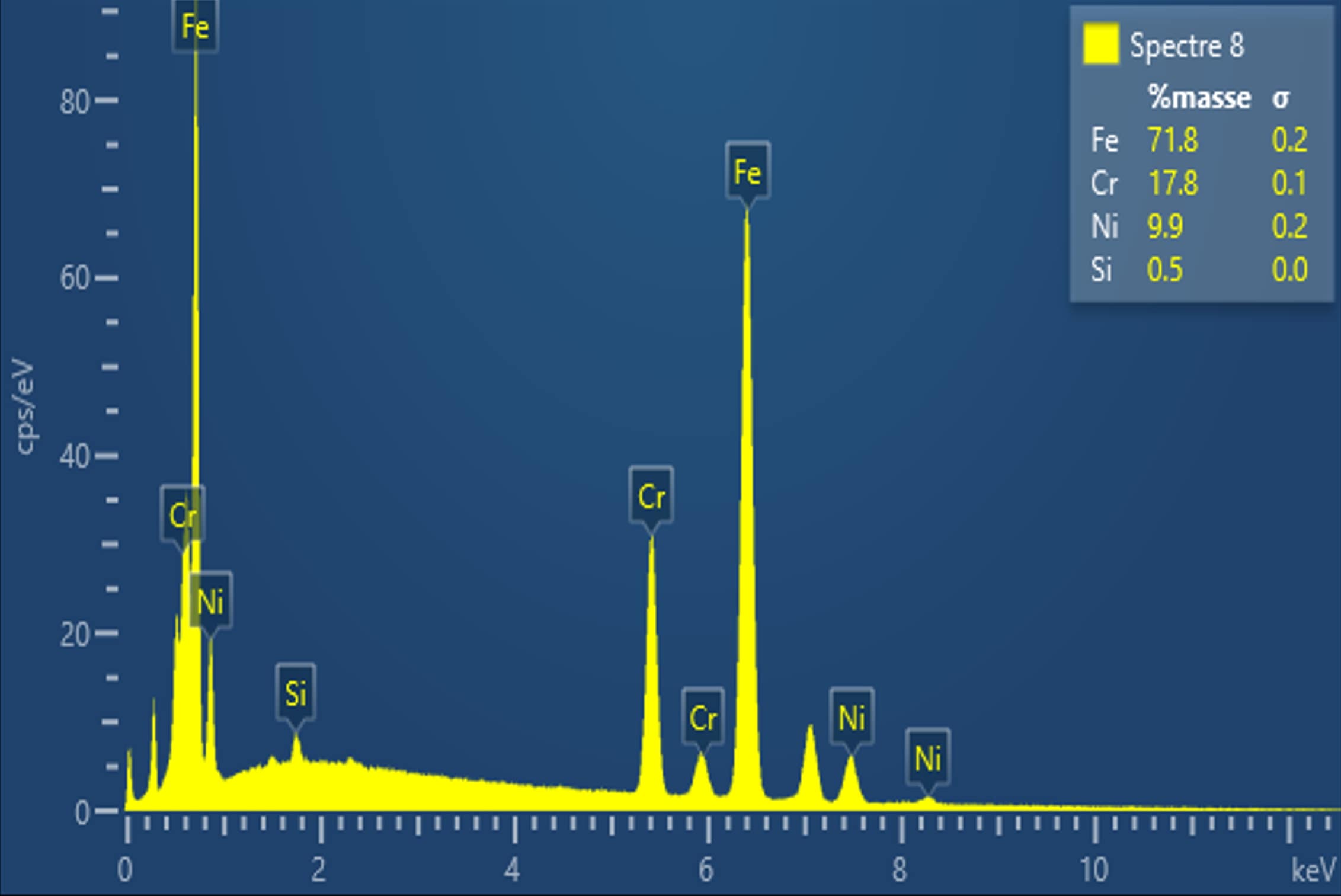
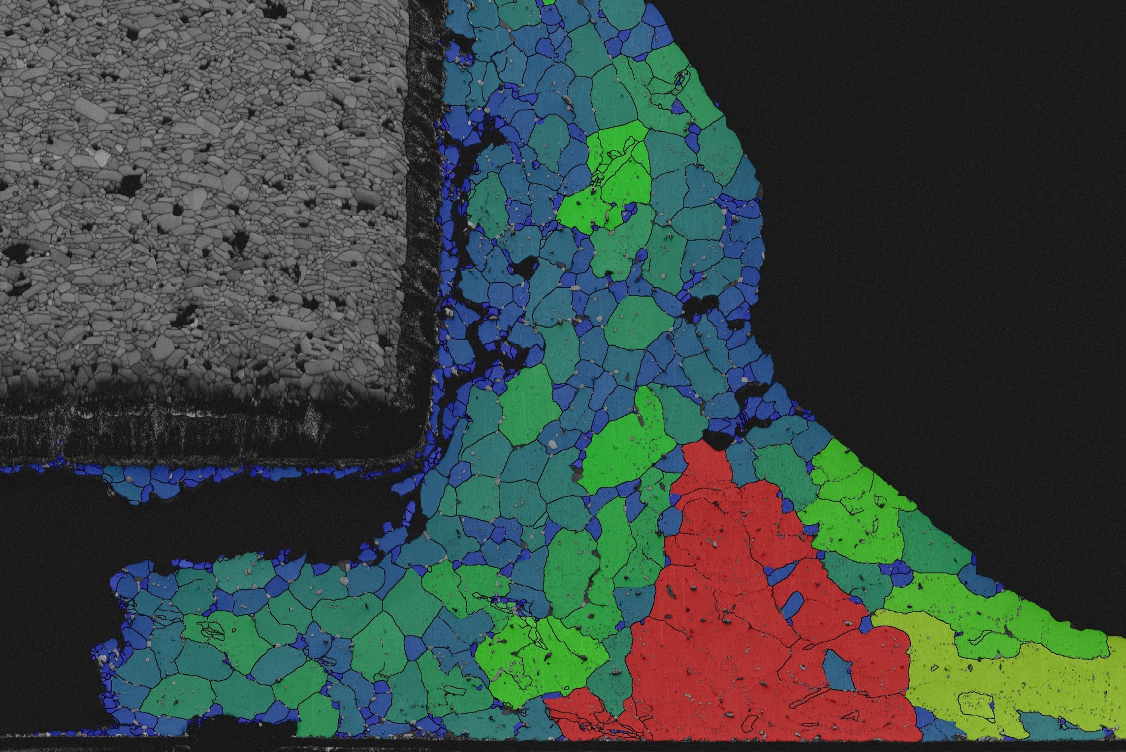
Surface analysis : composition, microstructure
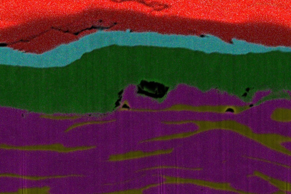
Mapping of the major elements (SEM-EDX)
Elementary spectrum: chemical composition (SEM-EDX)
Microstructure (SEM-EBSD)
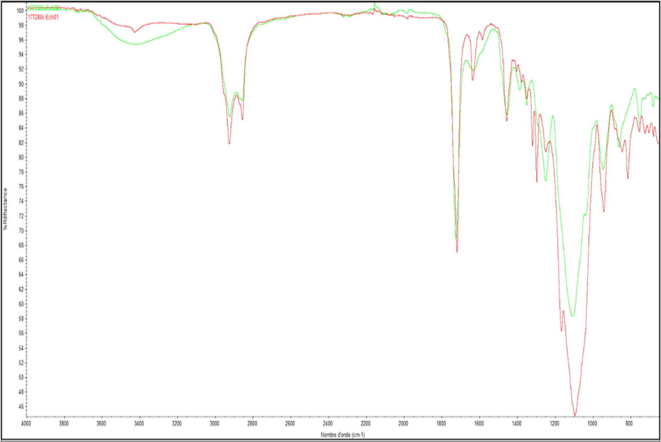
Molecular analysis (FT-IR)
Do you want a detailed presentation of our Lab services or consult us on a specific need ?